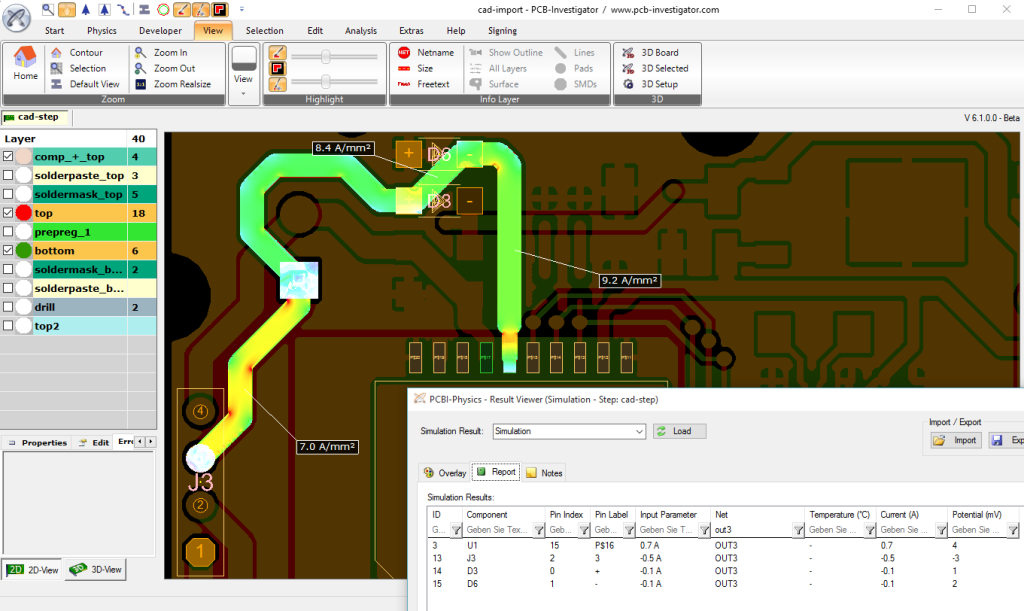
PCB Physics (Thermal Analysis / Current Simulation)
PCB-Investigator Physics is the perfect tool to simulate the physical behaviour of your Printed Circuit Boards during development phase.
It enables you to find thermal hotspots, critical trace resistances and voltage drops that are too high, even before prototyping begins!
With the built-in editing functions of PCB-Investigator Physics it’s even possible to optimize the layout and stack-up to achieve the best possible physical behaviour with only a few clicks!
Save valuable time and prototype costs with the Thermal Analysis and Current Simulation of PCBi-Physics! Get information about the physical behaviour of your Printed Circuit Board during operation, the Thermal Simulation and Current Flow Simulation of PCB-Investigator Physics enables you to simulate the following physical properties:
- The Temperature raise at each location caused by power loss of components or by high currents
- The Current Density, e.g. at copper bottlenecks or in drills
- The Voltage Drop and Copper Resistance between any pins on any layer
Simulation
In the area of simulation, the following areas can be checked:
- Temperature
- Voltage Drop
- Current Density
Manufacturing
In the area of manufacturing, the following areas can be reviewed:
- Plane Connections
- EMV Signal Tracking
- Copper Thickness
- Layer Stack-Up
Processing
In the area of further processing, the following areas can be checked:
- Ambient Temperature
- Heat Distribution Through Holes
Following up the causes of hot spots on printed circuit boards after the evaluation of a prototype and perhaps over several iterations of the “well-tempered” Board to approach, is expensive and complex. A thermal simulation that reduces these expenses, so far mostly the work of specialized physicist and part of the mechanical evaluation of PCB designs. PCB Investigator Physics (PCBi-Physics) now has a simulation tool used in the development and layout of phase to overcome with the thermal problems.
Which data is needed?
As input data you can select any CAD format supported by PCB-Investigator.
Supported formats are:
- ODB++
- GenCAD
- IPC2581
- IDF 2.0 / 3.0
- Gerber274x
Downloads
- White Paper
- Example Images
- Intro (Video)
Request a free quote
Please contact us to receive a non-binding offer
for the desired product.


