Hot Surface!
1) Introduction
For a battery-powered Motor, the DC battery current must be converted into alternating current (AC). In a compact manner, the conversion takes place on a printed circuit board with transistors, a control and monitoring processor (gate driver) adapted to the tasks and other sensor components. However, the power supply is not possible without losses, which heat up the assembly. The temperature does not only depend on the current, but this is one of the decisive factors.
In order not to have to take into account the electro technical details of the discharge process, the stand-by operation and the characteristic curves of the components [1], we simplify the examination and try to generate a temperature calculation only from the VM-GND circuit (see. Fig. 1) by numerical simulation.
For this purpose, PCB-Investigator Physics from EasyLogix is used.
Starting with CAD files in ODB++ format, it automatically shows a 3D model of the assembly, which must subsequently be provided with electrical and physical parameters, e.g., the material properties, currents and power dissipates.
Fig. 1: Block diagram of a battery-operated motor. Source: TEXAS INSTRUMENTS [1].
2) TI Sample Board
As an example, the 3-phase gate driver evaluation board BOOSTXL-DRV8304H from Texas INSTRUMENTS is used [2]. The board is 56 mm x 61 mm in size and has 4 signal layers (Fig. 2). The three discrete MOSFETS allow high power consumption and generate a lot of heat under these circumstances.


Fig. 2. Photograph of the BOOSTXL-DRV8304H by TI [2] (left) and PCB-Investigator model (right)
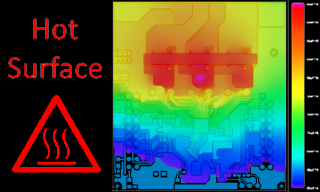
The top layer of the assembly is shown in Fig. 3. In this article, only the yellow bordered area is of interest, not least because of the striking label “Hot Surface”. How much °C and how many amperes “hot” mean is not further described in [2]. That’s why we want to find out whether it can really be so, with meaningful assumptions from the technical documentation [3]. “J1” is the connector (“Power”), that operates the power supply via VM+ / GND-.

Fig.3: Top layer of the TI evaluation board of DRV8304H, labeled with “Hot Surface”. Left: Technical documentation of TI [3], Right: PCB-Investigator ODB++ import.
3) Modelling
The geometric construction of the layers, prepregs and drills is done automatically from the ODB++ files. The physical circumstances (materials, environmental conditions, etc.) and electrical relationships (path of the current) are input variables.
3.1 Current path
PCB-Investigator Physics specializes in temperature calculation, based on the currents in the conductors and the power dissipation in the components. It is none and does not require circuit simulation a la SPICE. This allows great freedom in modeling, requires fewer input data and it is much faster. There are 2 ways to bring the electric heating into the model
Method 1: (Only) in the networks of interest, sources and sinks in the pads of the components define sectioned starting and stopping points for the current path.
Method 2: Components can be defined as current permeable and connect the sectioned starting and stopping points of the current path by so called pin-bridges.
3.2 Components
Again, there are 2 possibilities for heating.
Method 1: Direct input of power dissipation.
Method 2: If the component is used as a bridge between networks, the power can be implicitly defined via the electrical resistance of the component.
4) Model and results
The layer structure, traces and drills are imported from the ODB++ files and could even be modified afterwards in PCB-Investigator.

Fig. 4: Layer structure of the test board
The part of the circuit under discussion in this article is the path VM+ → GND- from connector J1, through the components U1, U2, U5 and R15, R29 and R33 and back (Fig. 5). We deliberately select a high RMS value of 30 A as the power requirement. As an electrical resistance of the U1, U2 and U3 we assume RDSON = 8 mΩ for high temperature and 7 mΩ for the 3 resistors [3]. For one and the same design, several so-called operation states can be created (by copying and changing) and calculated.
Fig. 5: The part of the circuit considered in this article: VM+ → GND−
4.1 Method 1: Sectional current path definition
PCB-Investigator knows the pads of the components and the networks that connect them. The input mask is used to indicate which networks are possible from component to component. After the choice of a network, the current can and must be entered [4]. The current situation is displayed immediately and the result shows Fig. 6. The advantage of this method is, that only certain parts of the layout can be calculated quickly and specifically without taking into account the connection with the rest of the circuit.

Fig. 6: Operation State of the current path from VM+ to GND− in Method 1. Each current path needs an ampere assignment and each component needs a power dissipation.
4.2 Method 2: Pin-Bridges
Only start and end pins receive the (total) current. The intervening nets and pads are “bridged” through the components in the algorithm [5]. How the current is then divided on the paths is determined by the (temperature depending) resistances of the components and the conductor paths. The power dissipation of the component is defined by itself during the calculation via the flowing current from I²R, plus additional losses added by the user. The advantage of this method is, that the total current for a new calculation can be varied very quickly.

Fig. 7: Current path from VM+ to GND− in method 2. Only the amperes of the total distance must be entered. The sections are “Auto”. Component losses are determined by the electrical resistance.
4.3 Result of the current flow
With both methods, the same electrical flow behavior is available as a result (Table 1). Because the inner signal layers are thinner than the outer signal layers, the current density (A/mm²) inside is higher.
| Top | Inner 1 | Inner 2 |
|---|---|---|
 |  GND− |  VM+ |
Table 1: Current density and current direction
Nevertheless, the current in the individual paths differs slightly. With method 1, exactly 10 A flow in each path according to the input parameters. With method 2, the paths of the smallest resistance carry more current. Tab. 2 shows the current through the components. Through U5 the way is the longest.
| Component | Current Method 1 | Current Method 2 |
|---|---|---|
| J1 | 30.00 A | 30.00 A |
| U1 | 10.00 A | 10.18 A |
| R15 | 10.00 A | 10.18 A |
| U2 | 10.00 A | 9.98 A |
| R29 | 10.00 A | 9.98 A |
| U5 | 10.00 A | 9.84 A |
| R33 | 10.00 A | 9.84 A |
Table 2: Current flow through the components
4.4 Result of the temperature
For the temperature calculation, the ambient conditions must be specified. We choose 20 °C air temperature with free convection. The differences in the current flow can have an effect on the component heating and thus on the temperature because of I²R (Tab. 3). However, the differences are too small in the calculated project and are not noticeable in the plots. The plots in Tab. 4 show the upper 50 K. The middle component is warmer than its neighbors due to its location. The jump from yellow to green is caused by the horizontally running conductive paths, respectively their isolation distances.
On the whole, the calculated assembly temperature is 100°C. This confirms that the specified region can really become a “hot surface” at high currents.
| Method 1 | Method 2 | ||||
|---|---|---|---|---|---|
| Component | Power | Temperature | Component | Power | Temperature |
| R15 | 0.700 W | 97.01 °C | R15 | 0.724 W | 97.94 °C |
| R29 | 0.700 W | 99.02 °C | R29 | 0.697 W | 99.14 °C |
| R33 | 0.700 W | 95.85 °C | R33 | 0.676 W | 95.26 °C |
| U1 | 0.800 W | 97.18 °C | U1 | 0.827 W | 98.06 °C |
| U2 | 0.800 W | 98.61 °C | U2 | 0.796 W | 98.79 °C |
| U5 | 0.800 W | 95.60 °C | U5 | 0.773 W | 95.19 °C |
Table 3: Component temperature
 Top signal layer |  Bottom signal layer |
Table 4: Temperature distribution in the layers
Sources:
[1a] Texas Instruments. “Driving Motors in Battery-powered IoT Systems” by John Lockridge
https://www.allaboutcircuits.com/industry-articles/driving-motors-in-battery-powered-iot-systems
[1b] Texas Instruments. “How analog integration simplifies the development of engine control in the car”
Elekronik Praxis 06.07.2021 by Arun Vemuri
https://www.elektronikpraxis.vogel.de/wie-analogintegration-die-entwicklung-der-motoransteuerung-im-auto-vereinfacht-a-1037022
[2] Texas Instruments. “DRV8304H Three-Phase Smart Gate Driver Evaluation Module”.
https://www.ti.com/tool/BOOSTXL-DRV8304H
[3] Texas Instruments. SLVUB97–October 2017. BOOSTXL-DRV8304H EVM User’s Guide.
https://www.ti.com/lit/ug/slvub97/slvub97.pdf
[4] Easylogix. “Tutorial 6: Transient simulation with different operating states.”
https://www.youtube.com/watch?v=y7Q5UGt1TVk
[5] Easylogix. “Tutorial 7: PinBridges & Easylogix Part Library.”
https://www.youtube.com/watch?v=_mDVDZAIagU